Description
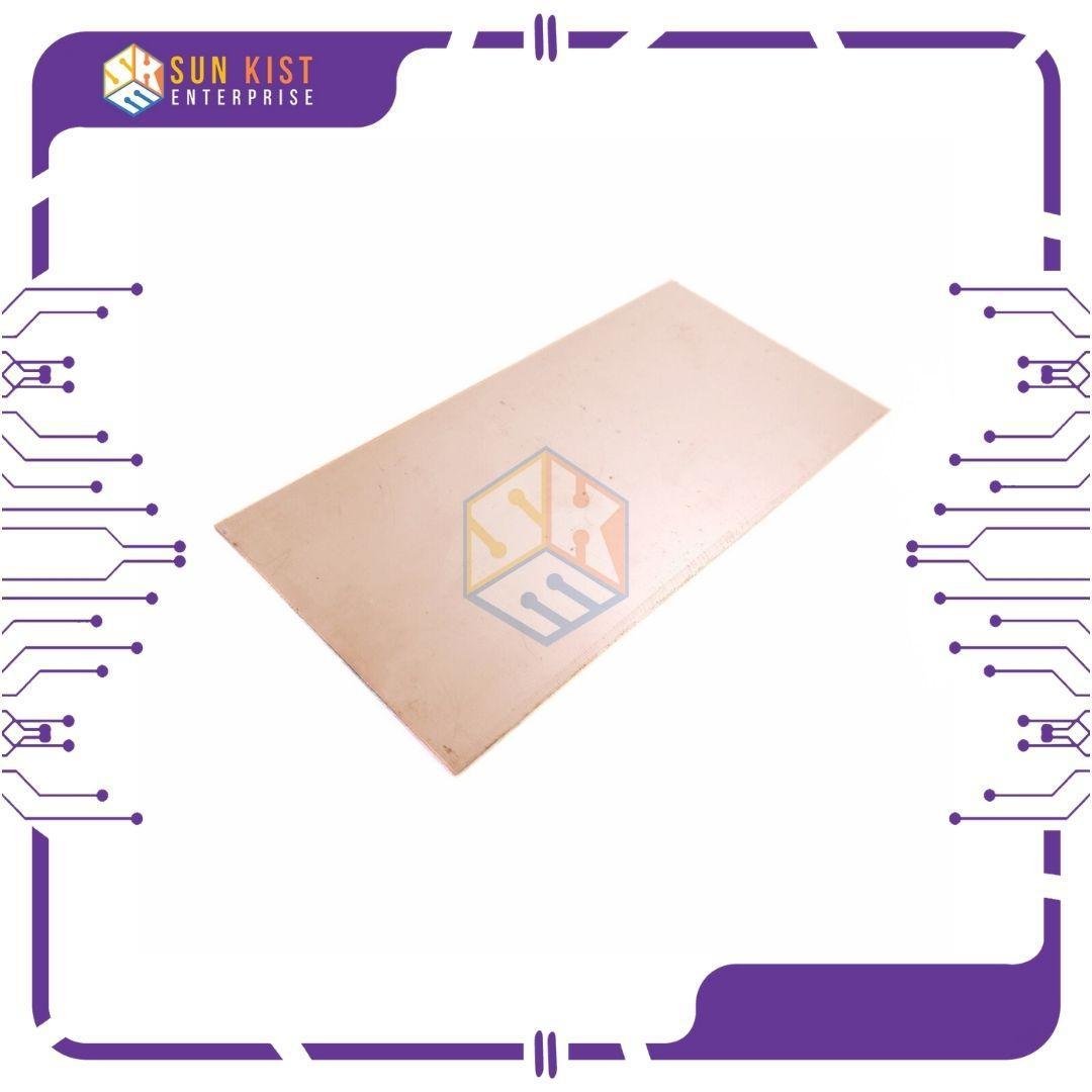
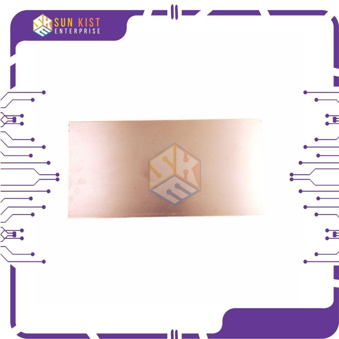
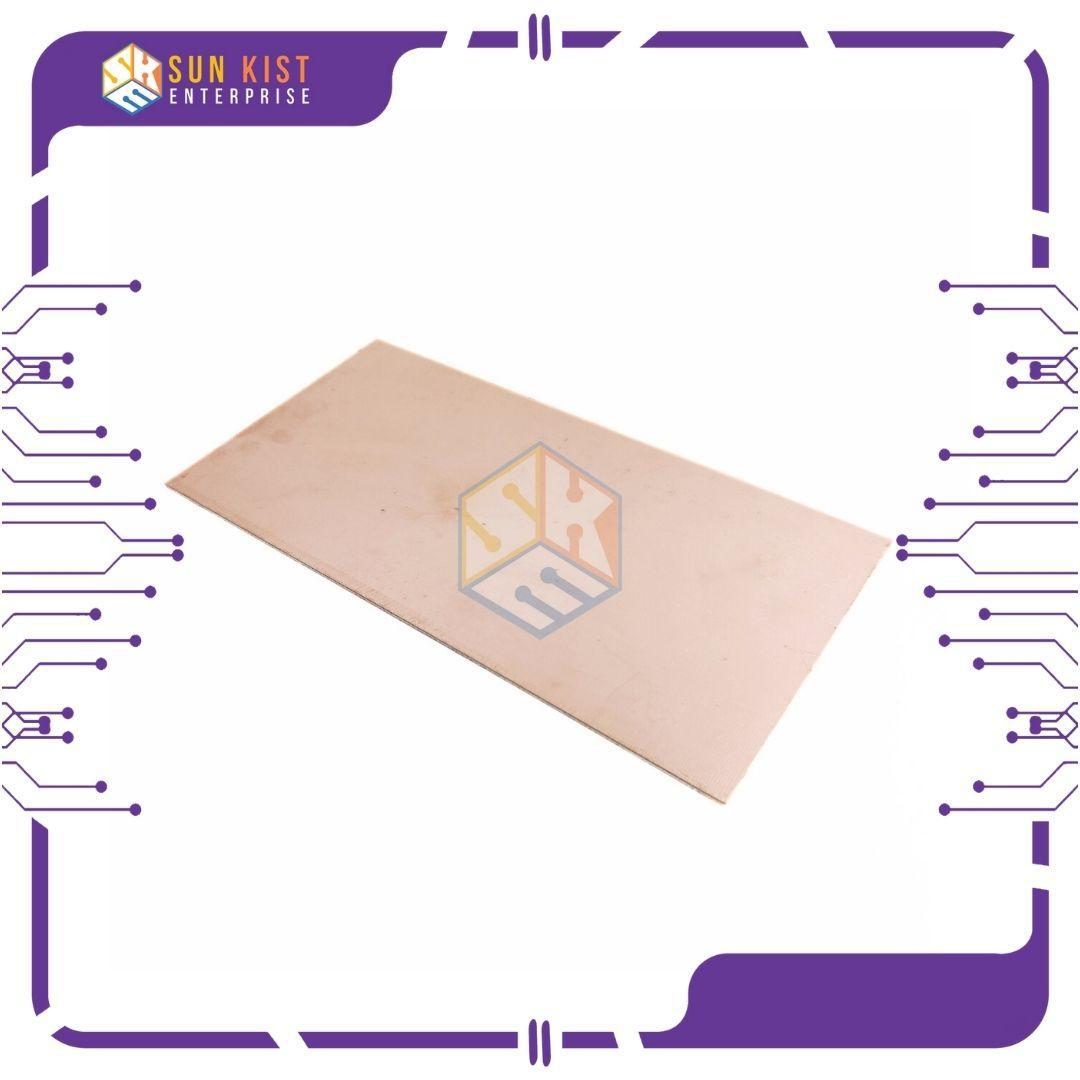
The description “10x20cm Double Sided Copper PCB Board” refers to a printed circuit board (PCB) with specific characteristics. Here’s a breakdown of what this description typically means:
Size:
The dimensions are specified as 10x20cm, indicating that the PCB has a rectangular shape with a length of 20 centimeters and a width of 10 centimeters.
Double Sided:
The term “double-sided” means that the PCB has copper traces and pads on both sides of the board. This allows for more complex circuit designs as components can be mounted on both sides.
Copper:
The PCB is made of a base material, often fiberglass (FR4), with copper layers laminated onto both sides. The copper is then etched to create the circuit traces and pads.
Purpose:
PCBs serve as the foundation for electronic circuits. They provide a platform for mounting electronic components and facilitate the electrical connections between these components.
Application:
PCBs are used in a wide range of electronic devices, from simple projects and prototypes to complex electronic systems. The specific application would depend on the circuit design implemented on the board.
Prototyping:
PCBs of this type are commonly used for prototyping electronic circuits. The 10x20cm size provides a reasonable amount of space for placing components and routing traces.
DIY Electronics:
Hobbyists and electronics enthusiasts often use such PCBs for their do-it-yourself (DIY) projects. They can solder components onto the board to create custom electronic devices.
Soldering:
The copper traces on the board are designed for soldering electronic components, such as resistors, capacitors, integrated circuits, and more.
Customization:
Users can customize and design their circuits on the PCB according to their specific project requirements.
Holes and Pads:
The PCB likely includes pre-drilled holes for component mounting and solder pads for making electrical connections.
When working with a PCB of this description, it’s important to follow good soldering practices and ensure that components are correctly placed and soldered. The layout of the traces on both sides of the board should be considered to avoid unintended short circuits. If specific design requirements or constraints exist for your project, always refer to the datasheet or documentation provided with the PCB or consult the manufacturer’s specifications.


